Curved image chip opens new possibilities
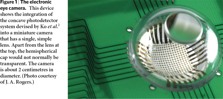
A collaboration of engineers from 6 different Midwest institutes led by John A. Rogers has published in the prestigious journal Nature, on a completed method for transferring planar formed circuit elements reliably and accurately onto a curved surface (Ko et. al., A Hemispherical electronic eye camera based on compressible silicon optoelectronics, Nature(London), (2008), 454(7): 748-753. Dr. Rogers has been researching stretchable ribbons and 2 dimensional sheets for the past few years that are designed to allow printed microfabricated circuits to be used in a wide variety of irregular surfaces such as “long term bionic implants, robotic sensory skins, ambient displays embedded in (for example) wallpaper, and intelligent surfaces that are chemically or electronically functionalized and can interact with people, objects or the environment.” The use of this technology to form an opticoelectronic imaging surface that mimics the animal retina (or the curved surface of a classical film cassette in a cassegrain astrograph) is a logical extension of this prior work. The current article in Nature heralds the successful demonstration of this principle.
In the article Roger’s group used a deformable elastomer in the shape of a small dome that was then stretched into to flat plane by the use of a jig clamped to the edges of the dome. A printed circuit array was formed on this flattened “drum head”. Each photo element (a Silicon P-n photodiode) was connected by specially designed compressible interconnecting ribbons to neighboring diodes. When the jig was released the elastomer reformed its dome shape, compressing the interconnecting ribbons that formed small arcs above the surface of the dome. This hemispherical array was glued to a concave glass lens substrate and the elastomer was peeled off leaving a concave hemispherical array of photodetectors. Simple arrays have been manufactured with 99 to 100% functioning pixels, but the pixel density and pixel count is far from that seen in modern imaging chips incorporated into current generation cameras. The limiting manufacturing aspects to this method involve connections at the periphery of the dome to a printed circuit board, a straightforward problem that will not impede further progress on improving numbers of pixels or pixel density. In fact, a very low number of pixels can yield a very high resolution image by eucentrically rotating the hemisphere, the same way biologic eyes function.
The advantages of using a hemispherical imaging chip were demonstrated in the article. The use of a very simple, single element lens produced excellent quality images without spherical aberration. No attempt in this article to address chromatic aberration was published. Refractive lens imaging was used in this article, but convex and concave surfaces for imaging could be constructed with this technique, so that a large number of optical systems might be simplified by including this kind of image chip. Even aspherical image surfaces could be manufactured, leading to exciting possibilities of using fewer optical elements, cheaper forms of glass, and suffering less transmission losses from fewer reflective surfaces. The possibility of a adaptive optical imaging chip that could dyanmically be deformed is even a conceivable future possibility.
In the article Roger’s group used a deformable elastomer in the shape of a small dome that was then stretched into to flat plane by the use of a jig clamped to the edges of the dome. A printed circuit array was formed on this flattened “drum head”. Each photo element (a Silicon P-n photodiode) was connected by specially designed compressible interconnecting ribbons to neighboring diodes. When the jig was released the elastomer reformed its dome shape, compressing the interconnecting ribbons that formed small arcs above the surface of the dome. This hemispherical array was glued to a concave glass lens substrate and the elastomer was peeled off leaving a concave hemispherical array of photodetectors. Simple arrays have been manufactured with 99 to 100% functioning pixels, but the pixel density and pixel count is far from that seen in modern imaging chips incorporated into current generation cameras. The limiting manufacturing aspects to this method involve connections at the periphery of the dome to a printed circuit board, a straightforward problem that will not impede further progress on improving numbers of pixels or pixel density. In fact, a very low number of pixels can yield a very high resolution image by eucentrically rotating the hemisphere, the same way biologic eyes function.
The advantages of using a hemispherical imaging chip were demonstrated in the article. The use of a very simple, single element lens produced excellent quality images without spherical aberration. No attempt in this article to address chromatic aberration was published. Refractive lens imaging was used in this article, but convex and concave surfaces for imaging could be constructed with this technique, so that a large number of optical systems might be simplified by including this kind of image chip. Even aspherical image surfaces could be manufactured, leading to exciting possibilities of using fewer optical elements, cheaper forms of glass, and suffering less transmission losses from fewer reflective surfaces. The possibility of a adaptive optical imaging chip that could dyanmically be deformed is even a conceivable future possibility.
Funding Member